M Baas
I am a machine learning researcher at Camb.AI. I post about deep learning, electronics, and other things I find interesting.
Building a simple charge pump with npn BJTs
by Matthew Baas
Building a simple charge pump with only resistors, diodes, npn BJT’s and capacitors.
TL;DR: For a course assignment I needed to construct a charge pump with limited components. I could not find any simple circuit online which used primitive components (no op-amps, no Schmitt triggers, no MOSFETs) and with an oscillator which cannot supply much current. So here is a design which I used, and it works reasonably well.
Background
Charge pumps are circuits which switch the orientation of capacitors rapidly to stack opposing capacitors up to one another to produce output voltages outside of the range of input voltages. e.g a charge pump with a 10V supply and a 5V oscillator could produce a -5V, -12V, or 30V output (of course the higher the voltage the harder the design for the same current). For this project I needed a charge pump inverter, which makes some \(V_{DD} > 0\) into some \(v_{out} < 0\). In this case, \(V_{DD} = 12\)V, while \(v_{out}= -5\)V.
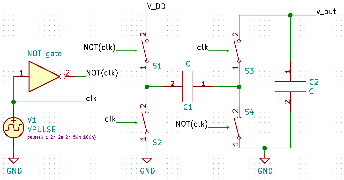
A minimal ideal charge pump inverting design has 4 switches which rapidly charge and discharge a capacitor which, for every half-cycle of the pulsed input, charges an output capacitor which smooths the negative output voltage. Such an idea example looks something like the image below. To get a feel for how it works please check out the wiki page or search “how do charge pumps work” in your favorite search engine.
The rest of this article will make the most sense if you have completed a university-level module or two in analog electronics.
Design
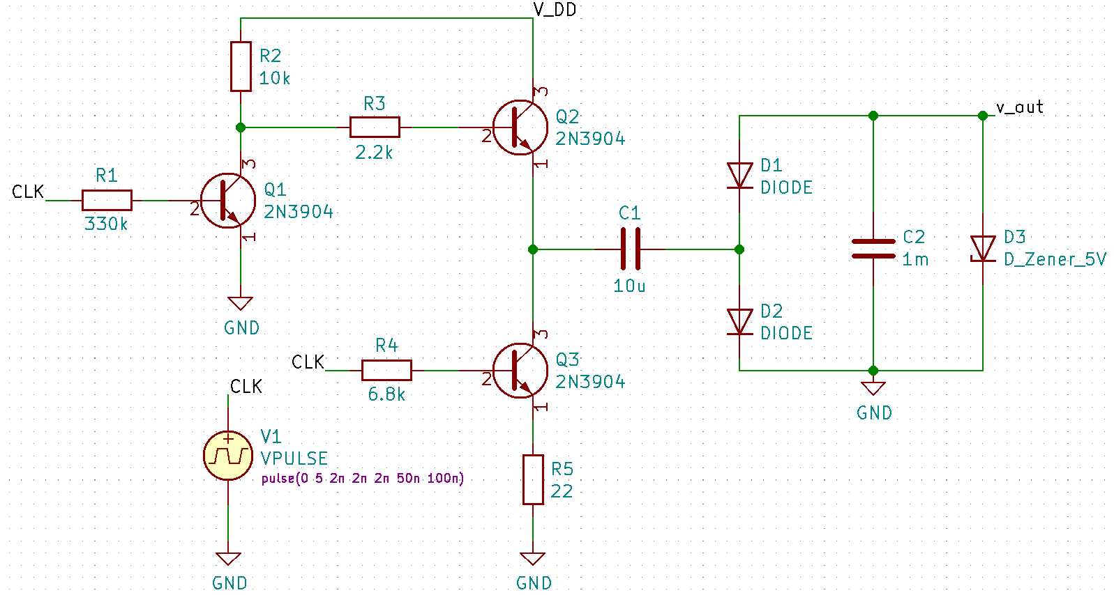
With such limited components, making switches and logical not circuits is not so trivial. The design is made to supply roughly 20mA. Since BJT and diodes are the only components that can act as a switch, I opted to make the design out of 3 stages:
- A common-emitter BJT amplifier that logically inverts the input signal (180° phase shift). This acts as the inverting not gate in the previous image.
- A power-amplifier-ish stage of two BJT transistors. This is because the 5V pulse train generated by oscillator might be a small IC or some other delicate circuit such that we can only really expect a few mA from it. These two transistors
Q2andQ3act as 2 of the switches in the ideal charge pump. - The capacitor actual-charge pump section. Here the two diodes act as the last two switches from the ideal charge pump figure. The big output capacitor ensures a low noise on the output, even when under a reasonable load. The circuit looks as shown below. When the ideal charge pump and the figure below are oriented in the same way it is easy to match up the components :).
Getting the values
To make the design much easier, we will assume a bunch of stuff. Then in the simulations we test to make sure our assumptions and design holds. For the resistors and capacitors, we only use the basic E12 series values.
Oscillator votlage and frequency
We do not want the frequency too high as that might increase noise or cause electromagntic interference if such a fast-switched signal is sent over a wire. It also shouldn’t be too low since then the output capacitor C2 needs to hold the negative -5V for longer before being topped up again. So a good middle ground is 1kHz to 10kHz. I picked 10kHz since it gave slightly less output noise in simulation.
Resistor values
- To find
R1, lets design the common-emitter amplification ofQ1to draw only 1mA when theCLKis high. Doing this, and assuming a \(\beta\) of 80 and a base-emitter on voltage of 0.7, we can write:
- To find
R2, we design the minimum collector voltage ofQ1as 2V (a good safety margin greater thanQ1saturation voltage of \(\approx\)0.3V). Then we can perform the calculation:
- Next
R5is added as an emitter resistor toQ3. It is added to both limit the current slightly whenC1is discharging and to make the amplifier stage slight more invariant to changes in \(\beta\) since the transistors practically used are not matched and can have substantially different current gains. To make sure it doesn’t mess up the AC characteristics too much, we keep it small and design the maximum voltage lost overR5to be 1V. Then we design the maximum discharge current throughQ3to be roughly 50mA (so that its RMS, since it is switched at 10kHz, is near the required 22mA we designed in the load). This allows us to state:
- Finding
R4then directly follows when using a \(\beta = 100\) (since the higher current will likely increase the gain slightly). So, again taking a base-emitter on voltage of 0.7V:
R3is added to limit the charging current whenQ2is conducting. I picked a value of 2.2k\(\Omega\) to limit the charging current to roughly \(\frac{12 - 0.7}{10\text{k} + 2.2\text{k}} = 92\text{mA}\) even at full load when the capacitorC1discharges completely during each half-cycle. This is not a super concrete way of finding the perfectR3, but it is a good rough guideline that seemed to hold up and work well in simulation.
Capacitor values
To draw a 20mA current from the -5V output, the effective load is roughly 220\(\Omega\). If we make the design decision that C is only to discharge lightly each half-cycle even at full load, we can let its time discharge time constant \(\tau = RC = 10(D_1 \text{ conducting period})\) so that it discharges a tenth of a time constant each half-cycle. Then we can equate:
To be on the cautious side, we pick C1 = 10μF. Next C2 is set to 1mF to keep the ripple voltage much less than 10mV. We can use the equation for the voltage ripple of a half-wave rectifier to get a rough approximation:
To be super safe, since we made tons of approximations, we choose a 1mF capacitor. You might also want to add a few small 150nF capacitors in parallel, since large 1mF capacitors generally have a substantial ESR (equivalent series resistance) which reduces its ability to attenuate high frequency noise.
So boom. Done :).
Simulation
It works pretty well. You can try build it in kicad/ltspice yourself and try it out. Below I show my plots for LTspice. The first figure below shows the transient response of the -5V output voltage when the circuit is under no load and under a full load drawing 22.7mA.
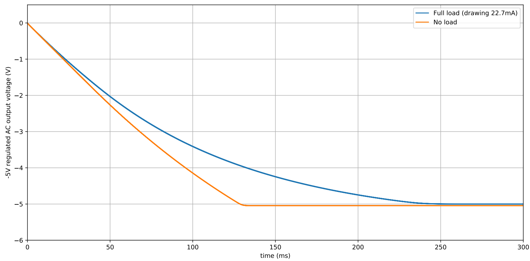
As is seen, the loaded transient response is quite long, however this is not a major concern since only the steady-state of a source matters in most cases. The figure also shows that the loading effect is not significant even when drawing a reasonable current, with the output voltage remaining near -5V. So looks good so far. The next figure below shows the transient response of the AC coupled noise on the output signal.
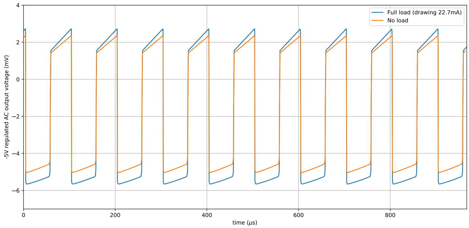
The noise is quite reasonable – remaining under 10mV peak-to-peak noise even at full load. So we can be pretty happy that most components using the -5V will not complain and work as intended. With that the simulations seem to indicate that the design works. Cool.
Practical Testing
Ok so its designed, simulated, now the proper test is actually building it and seeing if it works. So I built it using the components in the earlier schematic and plotted the DC output and the AC noise again using an oscilloscope. The DC output when the charge pump is loaded to draw roughly 12mA is show:
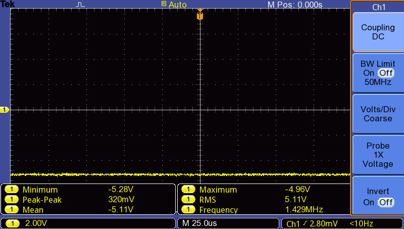
And look at that – the mean is just under -5V as expected when not significantly loaded. The design and simulations worked and we are nearly sorted. Lastly, I looked at the AC coupled noise (again when the charge pump was under a load drawing 12mA) to see if it is also reasonable:
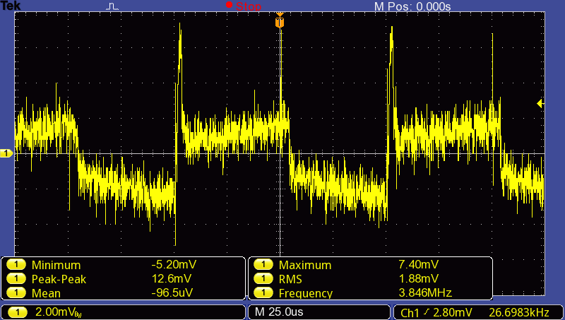
The peak-to-peak noise is still near 10mV as simulated! Nice. Further, the noise has a clear frequency of 10kHz, which corresponds to the switching frequency of the source. Using a more ideal source would decrease this noise. I did a little more testing when trying to draw the full 22mA, however the loading effect was quite a bit more than the simulation, with the output voltage falling to -4.7V. I suspect the reason for this is the capacitor values often have a large tolerance which could change up our calculations quite a lot, not to mention all the assumptions made during design.
Wrapping up
Overall, even though the practical circuit performed slightly worse than the simulations and design, it still performed quite well and is able to serve as a good -5V supply for low-current drawing applications (like a negative supply rail of an op-amp, or for negative voltage biasing of other circuitry). So hopefully if you needed a decent place to start for a BJT charge pump with minimal components, this circuit design will serve as a decent starting point. Of course if more ideal components (diodes/BJTs/low tolerance capacitors/resistors) are available, the performance will be even better and match more closely with the ideal design assumptions.
Notes
- Disclaimer: the method used to design the charge pump, and the circuit design itself uses many assumptions and approximations. It almost certainly will not work out of the box for any circuit configuration if the component values are not tweaked. It might, but no guarantees.
- I used KiCad for the figures and quick designing, then later ported them to LTspice for a more thorough simulation. KiCad has a great modern interface and controls, and offers much more than just schematics and simulation, but its simulation capabilities and interface are not as developed and feature rich as LTspice just yet (2019 Aug). Things like plotting power dissipation, SPICE
.meascommands, and current plots into different ports of a subcircuit are substantially easier in LTspice.